Ground FPGA Receiver
The signal receiver on the OGS is developed using an FPGA to receive data at high speeds.
A Digilent Zedboard with the Xilinx Zynq-7000 dual FPGA-CPU system allows the use of the chip’s FPGA to perform high-speed reading from the board’s input pins to the board’s DDR3 memory. Then, a loop on the CPU retrieves the updated data from memory and transmits it over Ethernet to the ground control computer.
We connect the comparator circuit with the FPGA Mezzanine Card (FMC) port on the right of the board, and output data over TCP using the Ethernet port on the board.
At the moment, we are using the XM-105 FMC expansion card to break out the pins on the FMC connector, allowing us to connect the FMC connector to the outputs of the comparator circuit. In the future, we plan to design a PCB for the comparator circuit which includes the FMC connector directly.
FPGA Logic
The following image shows a simplified block diagram of the design of the FPGA system.
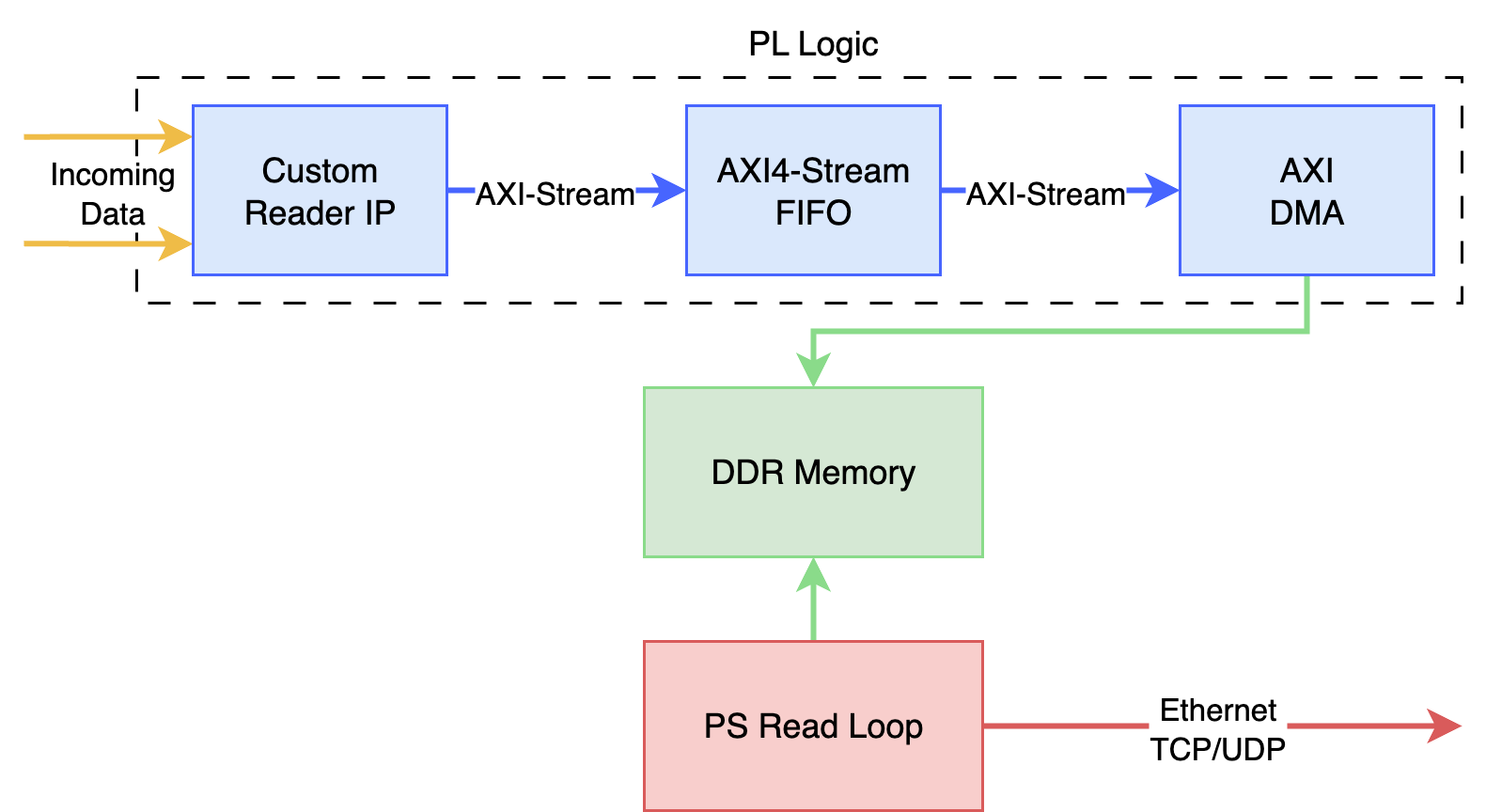
First, a custom module written in HDL (Verilog) will take in two input wires constrained to the inputs from the comparator circuit and decode the protocol one byte at a time, writing the data to an AXI-Stream port. Then, an AXI4-Stream FIFO IP is used to buffer the incoming data before going to an AXI DMA IP.
The FIFO is configured to output the TLAST signal every N number of bytes, which causes the DMA to write the new bytes to an N-byte wide section of memory. Once the transfer is complete, an interrupt is send to the PS.
The PS runs an TCP server which accepts clients from the network. When an interrupt signal is recieved from the PL, the TCP server broadcasts the recieved data to all connected clients. We choose a packet width N sufficiently large such that a TCP transfer can complete before the next interrupt is issued.
Protocol and Clock Synchronization
A central problem in all communications systems is synchronization between the transmitter and reciever clocks. To aid in clock synchronization, we intend to design a protocol incorporating a short preamble sequence at the start of each packet.
At the moment, we are developing the FPGA system to anticipate using a UART-like protocol, with an idle 1 state, a 0 start bit, and a return to idle for a stop bit, with an 8-bit word.
However, we may transitition to using a multi-bit 10101010 alternating sequence as a preamble to allow for clock synchronization and a longer word length, allowing for higher data density.