FPGA
Purpose
The FPGA will be used for laser modulation and formatting the data into an appropriate signal with respect to the transmission protocol. It will interface with the flash memory chip used by the payload controller over SPI, and output to the laser driver.
Technical requirements
-
Programmed in the Verilog HDL (Hardware Description Language)
-
Low latency reaching target modulation at 1-10 MHz
-
Space-grade: FPGAs are especially vulnerable to SEE (single event effects) like bitflips, because bitflips can affect the logical configuration directly. In LEO environments like those of our CubeSAT, we are Level 1 IEEE 1156.4-1997, or about 0.1 krad/yr.
Background
An FPGA is a programmable integrated circuit that directly implements digital logic using lookup tables and routing logic. A custom digital circuit can be programmed into the FPGA, and the FPGA directly implements that digital circuit in hardware, similar to an ASIC. For example, an AND gate can be implemented with a lookup table that outputs “1” when two inputs are “1” and “0” otherwise. The high-level architecture of an FPGA is thus a 2d-grid of lookup tables connected by routing logic, where both the lookup tables and the routing logic are configured to implement a program. The computational logic is first written in a HDL like Verilog, and this is then synthesized into a netlist, which is a representation of the logic gates needed to implement the logic. This is then implemented into a bitstream, which describes how the FPGA should be configured. Synthesis is analogous to compilation for programming languages, but it is a much more complicated and time-consuming process. Common synthesis software include Xilinx ISE, Xilinx Vivado, and Quartus. The largest FPGA brands are Xilinx (AMD), Altera (formerly Intel), and Lattice Semiconductor.
The FPGA’s use-case is as an intermediate between CPUs and ASICs, making it useful for specialized or singular applications. The FPGA’s main benefit over a normal CPU microcontroller is its extremely low latency, due to it directly implementing digital logic in a parallel manner, as opposed to CPUs, which sequentially execute a certain set of instructions. The FPGA’s main benefit over an ASIC is that it is reprogrammable, which is important for space applications due to the vulnerability of integrated circuits to radiation, and also its cost, since it is far cheaper and faster to program an FPGA than to custom-design an ASIC.
FPGAs have been extensively used on spacecraft for low-latency applications since the space industry only requires a small quantity of highly specialized circuits, so it would not be economical to use ASICs. In space, they are most commonly used in communications, digital signal processing, and highly parallel workloads like machine learning inference and computer vision.
FPGA Logic
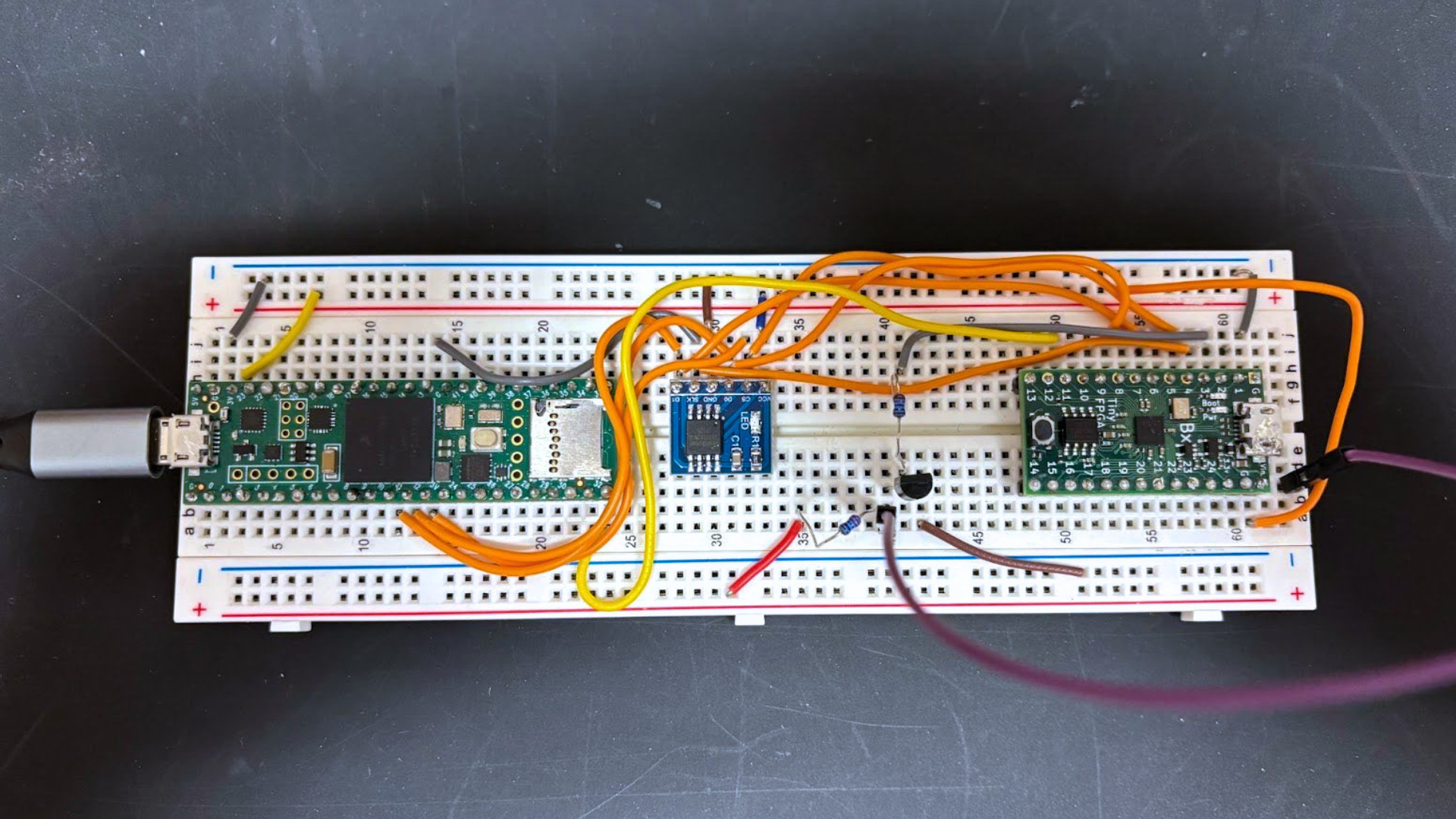
The FPGA’s logic is implemented in Verilog as a state-driven logic system that interfaces with the external flash memory. When a begin_send signal is sent and the payload controller relinquishes control, the output drivers are activated and a LED indicator is activated. The FPGA then uses either a 10MHz or 8kHz internal clock. It serially transmits an 8 bit instruction over IO0 while reading data in from IO1. After transmission, all outputs are returned to high impedance.
Options considered
-
VIRTEX-5QV FPGA Space-grade, radiation-hardened Extensive flight heritage https://www.wpafb.af.mil/News/Article-Display/Article/399355/novel-technology-takes-great-step-forward-with-success-in-flight/ https://www.electronicspecifier.com/industries/aerospace-defence/hundreds-of-space-grade-fpgas-deployed-in-satellite-launch Professional development IDE (Xilinx Vivado) and support
-
TinyFPGA BX dev board with a ICE40LP8K FPGA Open-source development board and toolchain for compiling and uploading Cheap, small footprint of ready-made board Currently used for testing, limited vendor support